Unveiling High NA EUV | ASML
ASML1 HN recommender · recommended in 1 month, 2024–2025
demo · general · 2024–2025 on HN
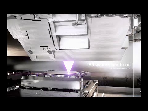
ASML's short promotional fly-through of its High NA EUV lithography platform, the TWINSCAN EXE, which supports 8-nanometer resolution. It shows the machine's internals including advanced anamorphic optics.
HN links it to show the sheer complexity of EUV machines, especially when discussing whether competitors can challenge ASML.
Up next
 5 mo on HN
38C3 - From Silicon to Sovereignty: How Advanced Chips are Redefining Global Dominance
media.ccc.de
5 HN recommender · 2025–2026
 18 mo on HN
Indistinguishable From Magic: Manufacturing Modern Computer Chips
Andor Gafotas
19 HN recommender · 2016–2024
 8 mo on HN
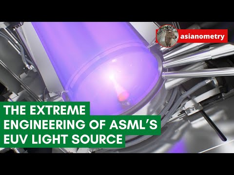
The Extreme Engineering of ASML’s EUV Light Source
Asianometry
11 HN recommender · 2022–2025
 8 mo on HN
Jim Keller: Moore's Law, Microprocessors, and First Principles | Lex Fridman Podcast #70
Lex Fridman
8 HN recommender · 2020–2023
 8 mo on HN
Jim Keller: Moore’s Law is Not Dead
UC Berkeley EECS
7 HN recommender · 2019–2025
 7 mo on HN
Why It Was Almost Impossible to Make the Blue LED
Veritasium
10 HN recommender · 2024–2026
 5 mo on HN
The man who almost faked his way to a Nobel Prize
BobbyBroccoli
6 HN recommender · 2022–2023
 5 mo on HN
AWS re:Invent 2016: Tuesday Night Live with James Hamilton
Amazon Web Services
5 HN recommender · 2016–2023
 4 mo on HN
How does Computer Memory Work? 💻🛠
Branch Education
5 HN recommender · 2022–2023
 4 mo on HN
"Z2" - Upgraded Homemade Silicon Chips
Sam Zeloof
4 HN recommender · 2021–2026
 4 mo on HN
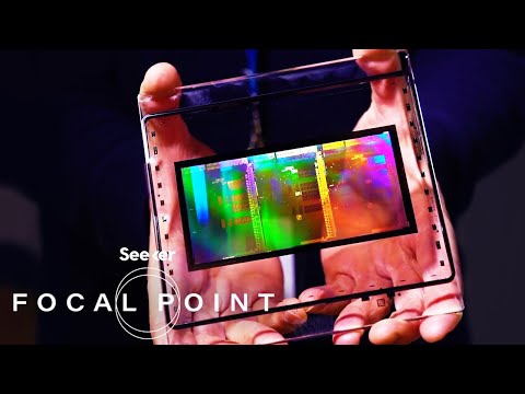
The Extreme Physics Pushing Moore’s Law to the Next Level
Seeker
5 HN recommender · 2019–2023
 4 mo on HN
Building a 6800 CPU on an FPGA with nMigen (part 1)
Robert Baruch
3 HN recommender · 2020–2021
4 comments from Hacker News
LOL, I recommend highly to everyone who thinks a startup can challenge ASML this 1.38min video: ▶ this video Its an industrial flight video through a ASML TWIN Exe HighNAV. Here is also a presentation of ~45min at CCC / Germany (in English language) which I highly recommend to watch: link Especially the explanation how they use two milisecond laser shots to first molt the tin and then distribute it symetrically(!!!) with a second shot across the surface. There IS NO chance that this startup will be able to somehow compete, if even Chinese state actors cant do it (yet).
The rest of the machine is no less incredible - the EUV light is reflected off a series of mirrors (the largest weighing, IIRC, somewhere in the region of 300kg, and the largest that Zeiss have ever made) onto a mask of the target pattern, which is rapidly shuttling back and forth, onto another series of mirrors, and finally focused onto the wafer stage, which is also moving precisely in step with the mask, to expose the photoresist on a single die which is on the order of 10mm square. And each wafer goes through multiple cycles of this, so not only does the machine rapidly create features at the nanonmetre scale with incredible accuracy, but again and again in exactly the same place after removing and returning the wafer. Oh, and the wafer stage is pretty fun too; it uses an electrostatic chuck that induces a charge in the wafer and therefore holds it firmly in place without needing any kind of suction that could distort the wafer. Promotional fly through video from ASML here: ▶ this video Asianometry video about the stage: link Another short video about the light source: link
Fly-through promotional render of the real thing: ▶ this video Incredible technology - the light-source works by generating droplets of molten tin, firing them through a chamber at around (IIRC) 200mph, and hitting each droplet with two laser pulses... at 50kHz. How they achieve that using Lego is beyond me.
I just found this one. ▶ this video Edit: I didn't realize that the droplets are hit twice by different lasers. link