The $200M Machine that Prints Microchips: The EUV Photolithography System
Branch Education3 HN recommenders · recommended in 3 months, 2025–2026
explainer · general · evergreen · 2025–2026 on HN
Branch Education's animated deep dive into ASML's EUV photolithography machine and how it prints nanometer-scale transistors onto chips. It covers the system's components and the process of chip manufacturing.
HN sends people here as the most straightforward and detailed starting point for understanding EUV lithography.
Up next
 6 mo on HN
The Battle of Midway 1942: Told from the Japanese Perspective (1/3)
Montemayor
7 HN recommender · 2019–2022
 3 mo on HN
Why Spotify Will Ultimately Fail
Benn Jordan
3 HN recommender · 2023–2024
 8 mo on HN
Brown; color is weird
Technology Connections
8 HN recommender · 2020–2026
 3 mo on HN
Small Planes Over Big Oceans (ETOPS Explained)
Wendover Productions
4 HN recommender · 2017–2020
 2 mo on HN
How does Starlink Satellite Internet Work?📡☄🖥
Branch Education
2 HN recommender · 2022–2024
 5 mo on HN
Big Plane vs Little Plane (The Economics of Long-Haul Flights)
Wendover Productions
8 HN recommender · 2017–2023
 5 mo on HN
Michael Stonebraker | Big Data is (at least) Four Different Problems
Michigan Engineering
5 HN recommender · 2015–2024
 4 mo on HN
The Ranks of Global Billionaires: Not All Billionaires Are Made Equal
Economics Explained
4 HN recommender · 2020–2022
 18 mo on HN
Indistinguishable From Magic: Manufacturing Modern Computer Chips
Andor Gafotas
19 HN recommender · 2016–2024
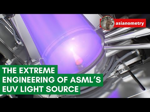 8 mo on HN
The Extreme Engineering of ASML’s EUV Light Source
Asianometry
11 HN recommender · 2022–2025
 8 mo on HN
Jim Keller: Moore's Law, Microprocessors, and First Principles | Lex Fridman Podcast #70
Lex Fridman
8 HN recommender · 2020–2023
 8 mo on HN
Jim Keller: Moore’s Law is Not Dead
UC Berkeley EECS
7 HN recommender · 2019–2025
4 comments from Hacker News
I'm always fascinated by how brilliant us humans can be. So much so that we can put billions of transistors in very small spaces and in complex structures while also mass producing it. I highly recommend watching this video about lithography and the machine that makes it all possible [1]. [1] ▶ this video
It’s a mind blowing achievement, nothing below sorcery if you think about it. ASML machines are hitting tin droplets with 25kW laser 50,000 times a second to turn them into plasma to create the necessary extreme ultraviolet light, and despite generating 500W of EUV, only a small fraction can reach the wafer, due to loses along the way. I believe it was like 10%. Here’s an incredible, very detailed video about it: ▶ this video
The Veritasium video is good but their "newscast" style with constant back-and-forth cuts to talking heads can make the presentation a bit disjointed. The more straightforward video of ASML EUV is from Branch Education: ▶ this video Because that vid gives an overview of the whole machine, it gives context to what each scientist is talking about in the Veritasium interviews.
Sure - once you have dozens of engineers and 5 years under your belt you'll be good to go! This will get you started: ▶ this video Keep in mind that every wafer makes multiple trips around the fab, and on each trip it visits multiple machines. Broadly, one trip lays down one layer, and you may need 80-100 layers (although I guess DRAM will be fewer). Each layer must be aligned to nanometer precision with previous layers, otherwise the wafer is junk. Then as others have said, once you finish the wafer, you still need to slice it, test the dies, and then package them. Plus all the other stuff.... You'll need billions in investment, not millions - good luck!