How are Microchips Made? 🖥️🛠️ CPU Manufacturing Process Steps
Branch Education2 HN recommenders · recommended in 2 months, 2024–2025
explainer · general · evergreen · 2024–2025 on HN
Branch Education walks through a semiconductor fab and the dozens of steps used to turn silicon wafers into microchips, with 3D animation. It covers lithography, deposition and etching at a high level.
Pointed to as a clear visual reference for chip manufacturing steps.
Up next
 3 mo on HN
The $200M Machine that Prints Microchips: The EUV Photolithography System
Branch Education
3 HN recommender · 2025–2026
 18 mo on HN
Indistinguishable From Magic: Manufacturing Modern Computer Chips
Andor Gafotas
19 HN recommender · 2016–2024
 8 mo on HN
The Extreme Engineering of ASML’s EUV Light Source
Asianometry
11 HN recommender · 2022–2025
 8 mo on HN
Jim Keller: Moore's Law, Microprocessors, and First Principles | Lex Fridman Podcast #70
Lex Fridman
8 HN recommender · 2020–2023
 8 mo on HN
Jim Keller: Moore’s Law is Not Dead
UC Berkeley EECS
7 HN recommender · 2019–2025
 7 mo on HN
Why It Was Almost Impossible to Make the Blue LED
Veritasium
10 HN recommender · 2024–2026
 5 mo on HN
38C3 - From Silicon to Sovereignty: How Advanced Chips are Redefining Global Dominance
media.ccc.de
5 HN recommender · 2025–2026
 5 mo on HN
The man who almost faked his way to a Nobel Prize
BobbyBroccoli
6 HN recommender · 2022–2023
 5 mo on HN
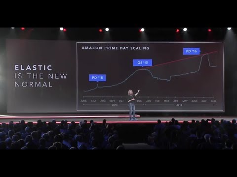
AWS re:Invent 2016: Tuesday Night Live with James Hamilton
Amazon Web Services
5 HN recommender · 2016–2023
 4 mo on HN
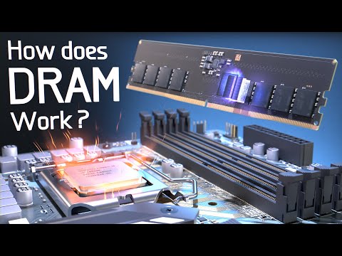
How does Computer Memory Work? 💻🛠
Branch Education
5 HN recommender · 2022–2023
 4 mo on HN
"Z2" - Upgraded Homemade Silicon Chips
Sam Zeloof
4 HN recommender · 2021–2026
 4 mo on HN
The Extreme Physics Pushing Moore’s Law to the Next Level
Seeker
5 HN recommender · 2019–2023
4 comments from Hacker News
Just to add to this, the Branch Education YouTube channel has great videos detailing the manufacturing process as well, here's one for starters: ▶ this video
In the description they say a video on lithography is on the way. In the mean time maybe this one from the same channel: ▶ this video Great channel
A video showing those steps, for the curious: ▶ this video It's probably not 100% identical to TSMC's process.
The graphic from the OIST in the link makes reference to both the reduced power needed and reduced capital costs, less mirrors & cheaper EUV light source. Also, less power -> less heat -> less cooling. I scoured for some other info as well: A single chip would go through a photo-lithography tool about 80 times. A photo-lithography tool can work on approx. 125 wafers per hour (5 FOUPS). A wafer contains ~230 chips. Current EUV light source requires a 20kw carbon laser. ▶ this video link